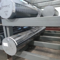
CZ-Silicon Crystals
Product Introduction:
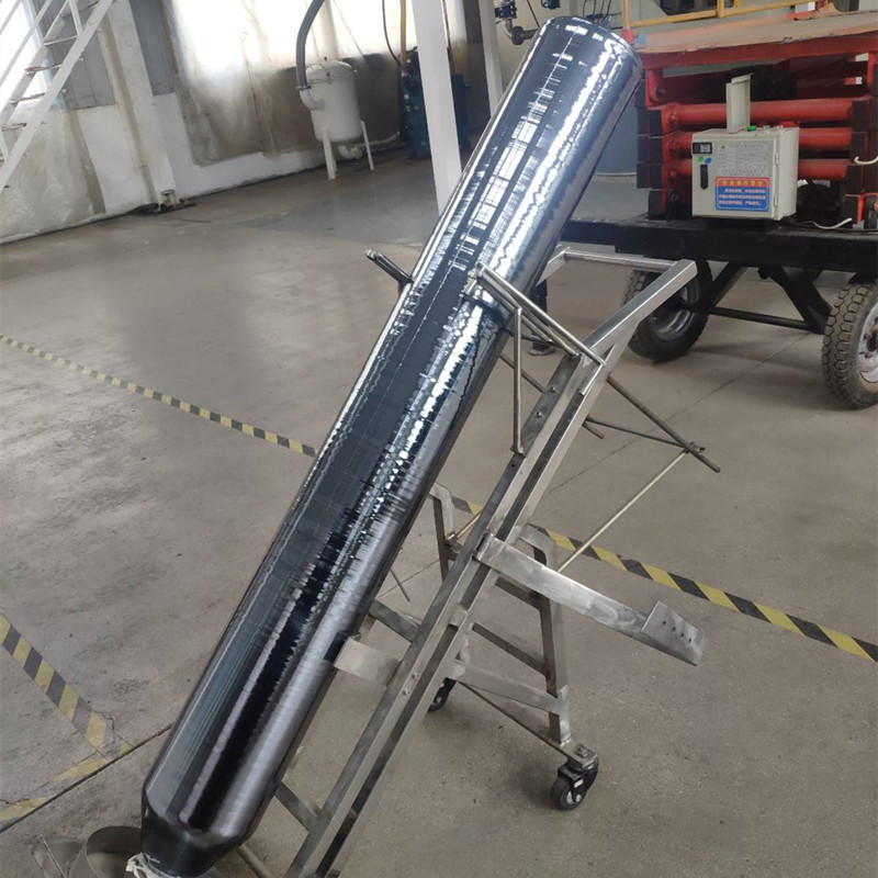
CZ silicon crystals are monocrystalline silicon grown by the cz method.Single silicon crystals are typically used in 3-5 μm mid-wave infrared optical windows and as substrates for optical filters.It is also commonly used for making laser mirrors due to its good thermal conductivity and low density.
We can provide various specifications of CZ silicon blanks and finished products. The shapes of blanks include round, rectangular, drilled, windows, lens, galvanometer,shaped, etc.
 CZ silicon crystals are monocrystalline silicon grown by the cz method.Single silicon crystals are typically used in 3-5 μm mid-wave infrared optical windows and as substrates for optical filters.It is also commonly used for making laser mirrors due to its good thermal conductivity and low density.Our company can provide many specifications of CZ monocrystalline silicon blanks and finished products.
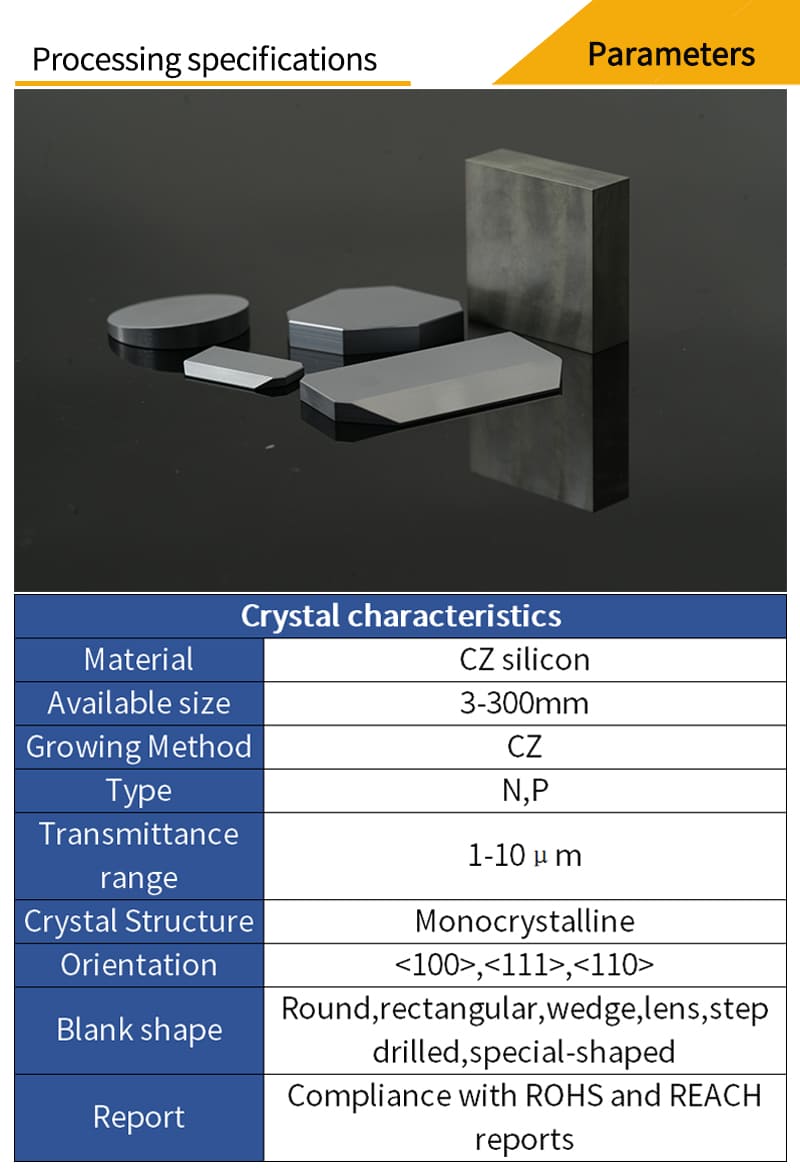 Our company can supply many specifications of single crystal silicon blanks and finished products.The shape of the blank contains round, rectangular, drilled, windows, lenses, galvanometers, special shaped etc.

Silicon has a high thermal conductivity and low density, making it suitable for making into laser mirrors. However, silicon is not suitable for CO2 laser transmission applications due to its strong absorption at 9 µm.
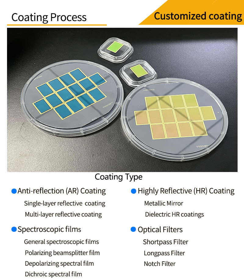
Coating refers to coating a transparent electrolyte film or metal film on the surface of the substrate material by physical or chemical methods. The purpose is to change the reflection and transmission characteristics of the material surface to reduce or increase the reflection, beam splitting, color separation, light filtering, polarization and other requirements.We can provide various optical coatings such as anti-reflective films, high-reflective films, spectral films, and metallic films. Broadband anti-reflective films are available for UV, visible, NIR and mid-infrared wavelengths.

Material Standards
●Material: Silicon single crystal with a chemical composition of Si
●Purity: The purity of the raw material used for crystal growth should be not
less than 9N (99.9999999%) and the purity of the dopant used should be not
less than 5N (99.999%).
●Crystallization quality: silicon single crystal rods should have no mosaic, no
grain boundaries, no twin crystals.
●Dislocation density: The dislocation density should be no more than 100
dislocations/cm2.
●Conductivity type: Silicon single crystal conductivity type of a total of two
types: N type, P type
●The crystallographic orientation of silicon single crystals consists mainly of
the following crystallographic directions

●Resistivity: The resistivity of silicon single crystals is divided into four classes.
●Appearance quality: no pollution, no chipping, no cracks, no holes on the
surface of silicon single crystal

Transmittance test
●Samples
Monocrystalline silicon, diameter not less than 20 ~ 50mm, thickness 10 ± 0.5mm,through the polished surface finish to 80/50
●Test band
3μm~15μm
●Qualification requirements
T≥52.5%@3-5μm
●N-BK7
N-BK7 is the most commonly used optical glass for processing high quality
optical components,, with excellent transmittance from visible to near-
infrared wavelengths(350-2000nm), and has a wide range of applications in
telescopes, lasers and other fields. N-BK7 is generally chosen when the
additional benefits of UV fused silica (very good transmittance and low
coefficient of thermal expansion in the UV band) are not required.
●UV fused silica
UV fused silica has a high transmission from the UV to NIR (185-2100nm).
In addition, UV fused silica has better uniformity and lower coefficient of
thermal expansion than H-K9L (N-BK7), making it particularly suitable for
high power laser and imaging applications.
●Calcium fluoride
Due to its high transmittance and low refractive index within a wavelength
of 180nm-8um, calcium fluoride is often used as windows and lenses in
spectrometers and thermal imaging systems. In addition, it has good
applications in excimer lasers because of its high laser damage threshold.
●Barium fluoride
Barium fluoride have high transmittance from the 200nm-11um and they are
resistant to stronger high-energy radiation. At the same time, barium fluoride
has excellent scintillation properties and can be made into various infrared
and ultraviolet optical components. However, the disadvantage of barium
fluoride is that it is less resistant to water. When exposed to water, the
performance degrades significantly at 500℃, but it can be used for
applications up to 800℃ in a dry environment. At the same time, barium
fluoride has excellent scintillation properties and can be made into various
infrared and ultraviolet optical components.It should be noted that when
handling barium fluoride material, gloves must be worn at all times and
hands must be washed thoroughly after handling.
●Magnesium fluoride
Magnesium fluoride is ideal for applications in the wavelength range of 200nm
-6um. Compared to other materials, magnesium fluoride is particularly durable
in the deep UV and far IR wavelength ranges. Magnesium fluoride is a powerful
material for resistance to chemical corrosion, laser damage, mechanical shock
and thermal shock. It is harder than calcium fluoride crystals, but relatively soft
compared to fused silica, and has a slight hydrolysis. It has a Nucleus hardness
of 415 and a refractive index of 1.38.
●Zinc selenide
Zinc selenide has high transmittance in the 600nm-16um and is commonly
used in thermal imaging, infrared imaging, and medical systems. Also, due to
its low absorption, zinc selenide is particularly suitable for use in high-power
CO2 lasers. It should be noted that zinc selenide is a relatively soft material
(Nucleus hardness 120) and is easily scratched, so it is not recommended for
use in harsh environments. Extra care should be taken when holding, and
cleaning, pinching or wiping with even force, and it is best to wear gloves or
rubber finger covers to prevent tarnishing. Cannot be held with tweezers or
other tools.
●Silicon
Silicon is suitable for use in the NIR band from 1.2-8um.Because of its low
density, silicon is particularly suitable in applications where weight
requirements are sensitive, especially in the 3-5um . Silicon has a Nucleus
hardness of 1150, which is harder than germanium and not as fragile as
germanium.It is not suitable for transmission applications in CO2 lasers
because of its strong absorption band at 9um.
●Germanium
Germanium is suitable for use in the near-infrared band of 2-16um and is well
suited for infrared lasers. Due to its high refractive index, minimal surface
curvature and low chromatic aberration, germanium does not usually require
correction in low power imaging systems. However, germanium is more
severely affected by temperature, and the transmittance decreases with
increasing temperature; therefore, it can only be applied below 100°C. The
density of germanium (5.33 g/cm³) is taken into account when designing
systems with strict weight requirements. Germanium lenses feature a
precision diamond lathe turned surface, a feature that makes them well suited
for a variety of infrared applications, including thermal imaging systems,
infrared beam splitters, telemetry, and in the forward-looking infrared (FLIR)
field.
●CVD ZnS
CVD ZnS is the only infrared optical material, other than diamond, that
covers visible to long-wave infrared (LWIR), full wavelength and even
microwave wavelengths, and is currently the most important LWIR window
material. It can be used as windows and lenses for high-resolution thermal
imaging systems, as well as for advanced military applications such as
"tri-optical" windows and near-infrared laser/dual-color infrared composite
windows.


